“First GaN to be introduced for mobile phone handsets in the world”, says
Jay Son, CEO of Innoscience
keyboard with phone and tablet pc
Innoscience Technology, a company founded to create a global energy ecosystem based on high performance, cost-effective Gallium Nitride on Silicon (GaN-on-Si) power solutions, today announced the INN40W08, a 40V bi-directional GaN-on-Si enhancement mode high-electron-mobility-transistor (HEMT) for mobile devices, including laptops and cellular phones. The INN40W08 HEMT has been developed using the company’s advanced InnoGaN technology which features ultra-low on resistance.
Commented Dr. Denis Marcon, General Manager of Innoscience Europe and Marketing Manager for the USA and Europe: “GaN technology has been adopted by manufacturers of mobile phone chargers over the last couple of years to deliver increased power and shrink device size. However, Innoscience’s significant breakthrough now makes it possible to introduce GaN HEMTs into mobile phone handsets as well, increasing efficiency and performance. With Innoscience’s huge available capacity, we provide the secure supply chain that customers nowadays expect.”
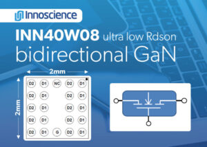
Featuring a bi-directional blocking capability, the new INN40W08 GaN HEMTs have a ultra-low on resistance of just 7.8 mΩ. This is achieved by the company’s advanced InnoGaN patented strain enhancement layer technology which reduces sheet resistance by 66%. Gate charge (QG) is typically 12.7nC. The 5×5 grid wafer level chip scale package (WLCSP) measures just 2×2 mm. This small footprint enables INN40W08 GaN HEMTs to be integrated inside mobile phones. Applications include high side load switching, over-voltage protection in a smart phone’s USB port and multiple power supplies including chargers and adapters. Innoscience’s GaN technology enables efficient and more compact over-voltage-protection (OVP) systems by replacing 2 Silicon MOSFETs with 1 InnoGaN (or BiGaN) transistor. This saves on the overall OVP costs and makes the OVP unit smaller, which is very important considering the space constraints on a mobile phone’s circuit board.
Innoscience is the world’s largest Integrated Device Manufacturer (IDM) that is fully focused on GaN technology. The company has two wafer fabs including the world’s largest dedicated 8-inch GaN-on-Si site. Currently the company has a capacity of 10,000 8-inch wafers per month which will ramp up to 14,000 8-inch wafers per month later this year and 70,000 8-inch wafers per month by 2025. The company has a wide portfolio of 30 – 150V and 650V e-mode GaN-on-Si transistors. Innoscience’s GaN technology has reached consistently high international standards including advanced qualifications and reliability testing.
About Innoscience
Innoscience is an Integrated Device Manufacturer (IDM) founded in December 2015 with main investment from CMBI, ARM, SK and CATL. With the development of new technologies, the electric power grid and power electronic systems across the world are undergoing a massive transformation. Our vision is to create an energy ecosystem with the most effective and low-cost Gallium-Nitride-on-Silicon (GaN-on-Si) power solutions. In November, 2017, Innoscience first established a mass production 8-inch wafer line for GaN-on-Si devices in Zhuhai. In order to fulfill the rapidly growing power demands, Innoscience has inaugurated a new facility in the Suzhou in September, 2020. As a cutting-edge GaN technology provider, Innoscience’s 1,400+ employees and over 300 R&D experts are dedicated to delivering high performance and high reliability GaN power devices that can be widely used in diverse applications including cloud computing, electric vehicles (EV) and automotive, portable devices, mobile phones, chargers and adapters. For more information, please visit http://www.innoscience.com.
Contact Media:
Peter Rogerson, Innoscience
+1 408-502-4626
Benoit Simoneau, 514 Media
+44 (0) 7891 920 370
